

ATmega4809 - An Introduction
The new ATmega4809 are part of the megaAVR-O line of processors with 48KB flash, 6KB SRAM, 256 bytes EEPROM with a clock of up to 20MHz. The new megaAVR-O series provides additional functionality including; an Event System, enabling direct peripheral-to-peripheral signaling, an Configurable Control System and a CRC System.
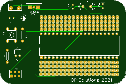
I've created a basic ATmega4809 development board and provided the gerber files as a download, figure 1 is an image of the board.
In this article we will be looking at some of the basic functionality of the new ATmega4809 AVR-O series chip. Mouser Electroincs have a limited quantity of these 40-pin PDIP devices listed at $2.84 as of this date 10/5/2021. mouser.com
I have made available gerber files for a BETA version of an ATmega4809 40-pin development board with; 5V regulator, reset button, an LED on port PA7 and space for a external crystal oscillator.
Unlike previous AVR version that use a debugWire to program and debug the chips the ATmega4809 uses a Unified Program and Debug Interface (UPDI) interface. A ISP like 6-pin header is provided on the board and an Microchip ICE can be used. A Link to an article describing how to create a UDPI programmer is provided below in the references.
Throughout this article frequent referrence to the ATmega4809 datasheet is made and can be downloaded from the Microchip web site scroll down to the documentation section.
Setting the Main Clock frequency
Referrirng to the datasheet, section 10.3.3 the Main Clock After Reset states that the CLK_MAIN is set to the 16/20MHz clock with a prescale factor of 6 which gives a clock frequency of 3.33 MHz. To change the default frequency at startup the OSCCFG fuse setting may be set to either 20MHz or 16MHz, it is 20MHz by deffault. To modify the prescale factor is not as simple as with previous AVR chips, an extra step is necessary. In order to protect certain registers from being overwritten an Confuration Change Protection scheme has been inplemented. (Refer to section 10.3.5)
Attempting to write to a protected register without following the appropriate CCP unlock sequence leaves the protected register unchanged. ATmega4809 datasheet
// Once the CCP register has bee written to the prescale value must be set
//  immediately after.
CCP = CCP_IOREG_gc;         // Key from table 10-1 section 10.3.5
CLKCTRL.MCLKCTRLB = 0;  // Main Clocik Control B register setion 10.5.2
I've just touched on the capablilities of the Clock Controller, section 10 in the datasheet provides an in-depth look at the inner workings and register settings for the ATmega4809.
Output main clock to external pin
When I first coded a blink application to get an understanding of th9is new chip the output didn't seem to be at the frequency I expected. I had only scanned over the datasheet and didn't realize that the main clock had a prescale factor of 6 so I wanted to output the clock to an external pin to see what I actually had.
CCP = CCP_IOREG_gc;     // Key from table 10-1 section 10.3.5
CLKCTRL.MCLKCTRLA = CLKCTRL_CLKOUT_bm;  // Section 10.5.1 Main clock A
Again the CCP register had to be set then the CLKOUT bit set in the Main Clock Control A register is set;
Working with GPIO
There are 33 General Purpose I/O pins available on the 40-pin PDIP package that may be used an digital I/O or multiplexed for some other purpose. Refer to Section 16 of the datasheet.
The ports are defined as;
- PORTA[0:7]
- PORTC[0:5]
- PORTD[0:7]
- PORTE[0:3]
- PORTF[0:6]
Manipulating the I/O ports on the ATmega4809 is handled a bit differently than the way it was done in the past but basically done the same way. Section 16 in the datasheet describe the registers and how they work so I'll just show by example how this is accomplished. We'll start off with the obligatory blink program.
#define LED_PIN	PIN3_bm

int main(void)
{
	PORTA.DIRSET = LED_PIN;   // Set PORTA.PIN3 to output

    while (1)
    {
		PORTA.OUTTGL = LED_PIN;    // Toggle state
        _delay_ms(200);
    }
}
In summary the new ATmegaAVR O-series chips, in my opinion have taken a leap forward and provide a much improved and intelligent design. I have found the ATmega4809 very easy to work with and look forward to using it in future applications.
References
Download Here